Split-flap build guide
From printed parts and bare PCBs to a working display. It follows David Königsmann's original instructions (Printables 69464) and his photos, changed for this build: shortened case, hand-soldered boards, and an ESP32 in place of the ESP-01. Hole positions and screw paths come from the CAD model. Pick your size at the top and every quantity updates. Ticks are saved in this browser, and Next step in the top bar jumps to the first step you haven't ticked. Steps with a 3D button show that step in the stage's 3D diagram. Click any photo to enlarge it.
Parts and fasteners
for 9 units| Printed | Qty |
|---|---|
UnitFrame | 9 |
FlapDrumInner + FlapDrumOuter | 9 each |
| Flaps, 45 per unit | 405 |
| Case: Left, Center, Right of MiddleFrame, FrontCover, BackCover | 9 pcs |
| Electronics | Qty |
|---|---|
| Bare PCB, Arduino Nano, 12 V 28BYJ-48, KY-003, 2×1 mm magnet | 9 each |
| ULN2003A (SOP-16), L7805CV, 4-position DIP switch | 9 each |
| 330 nF and 100 nF capacitors (0805) | 9 each |
| 1×15 female header | 18 |
| JST-XH board sockets: 5-pin, 3-pin | 9 each |
| JST-XH board socket: 4-pin | 18 |
| XH-4 cable, plugs on both ends, 100 mm (bus) | 8 |
| XH-3 cable, plug on one end, 300 mm (hall sensor) | 9 |
| XH-4 cable, plug on one end, 200 mm (power + ESP32) | 1 |
| ESP32 DevKit, BSS138 level-shifter module, 12→5 V buck | 1 each |
| 12 V ≥3 A supply, 1000 µF 25 V capacitor | 1 each |
| DC jack for a hole under 9 mm (the case hole is 9.2 mm) | 1 |
| KCD1-101 rocker switch (the case hole is 18.5×12.5 mm) | 1 |
| 22 AWG silicone wire, flux, double-sided foam tape | — |
| Fastener | Where | Qty |
|---|
Fastener assignments are from the upstream screw table. Per unit: 2 of each unit fastener. The case needs the same count for every size.
Tools
| Tool | Used for |
|---|---|
| Soldering iron with a fine tip, solder, flux | The boards and cables. At about 200 °C it also melts in the heat inserts |
| Multimeter with continuity mode | Board checks, the power lead, each bus cable, setting the buck converter |
| Screwdrivers or hex keys to fit your M2, M3 and M4 screws | Every fastener in the table above |
| Small screwdriver | The buck converter's trimmer and the DIP switches |
| Flush cutters, wire strippers, tweezers | Wires, and placing the surface-mount parts |
| Glue for the magnets, a marker, tape, labels | Magnets, marking the magnet's face, tagging wires and units |
| USB cables for the Nano and for the ESP32 | Flashing. Check which sockets your boards have |
PC with PlatformIO (pio) | Flashing and the serial monitor |
| Soft cloth, sandpaper or a knife | Protecting the case faces, trimming seams that don't close |
What each printed part looks like

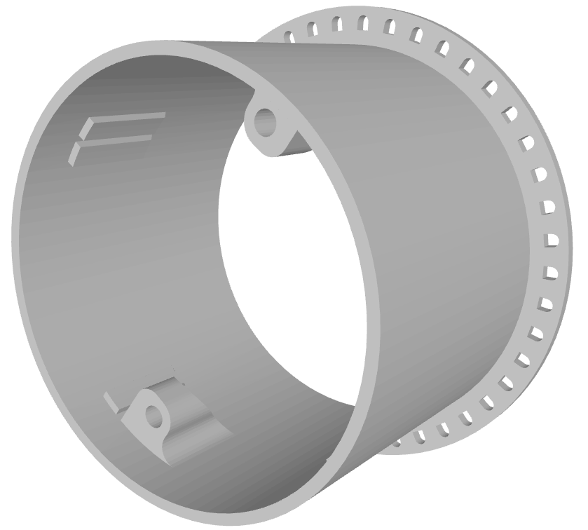
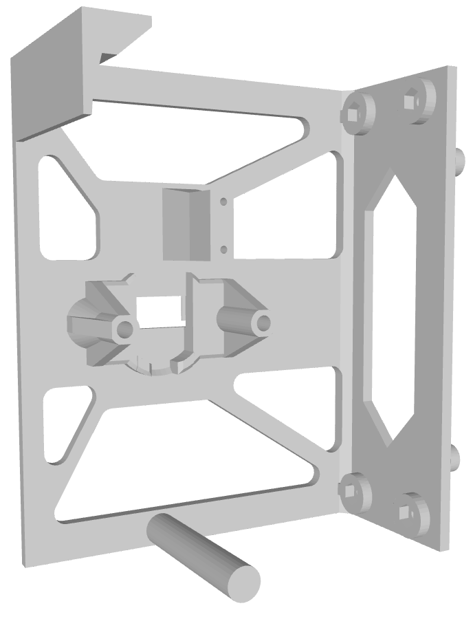
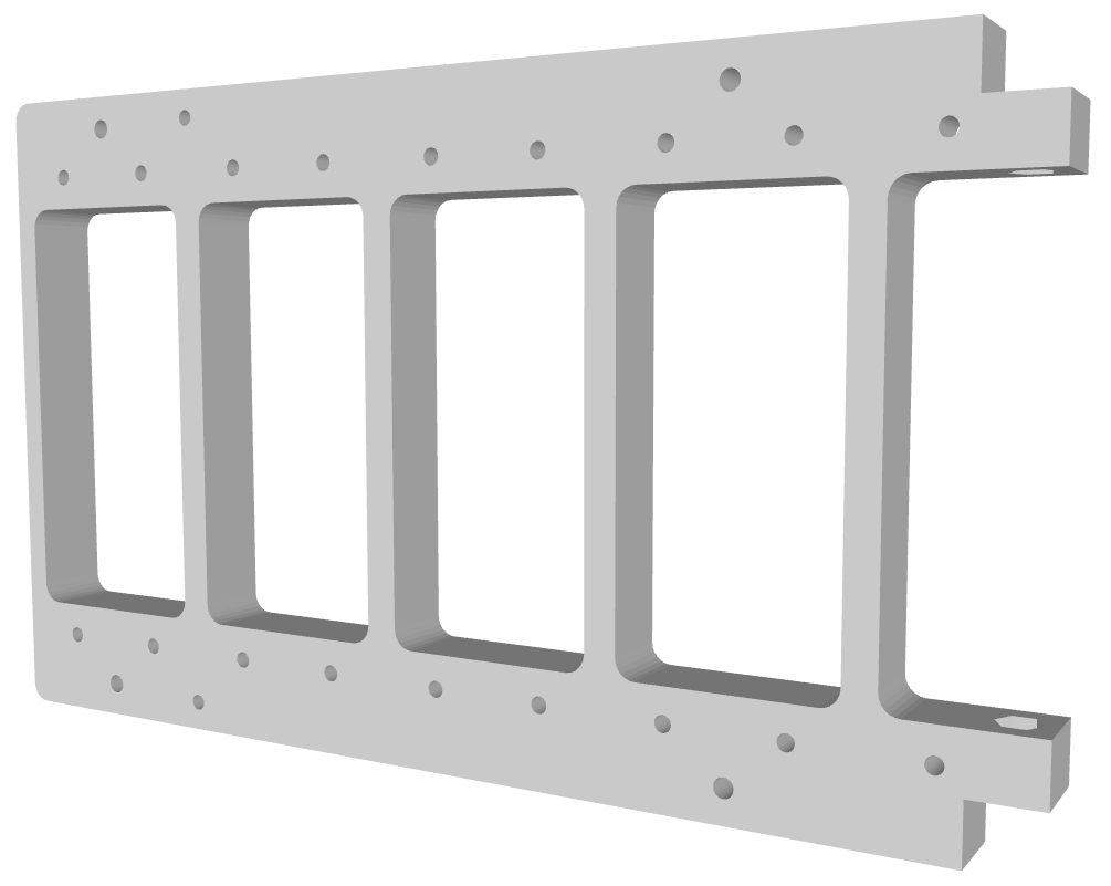
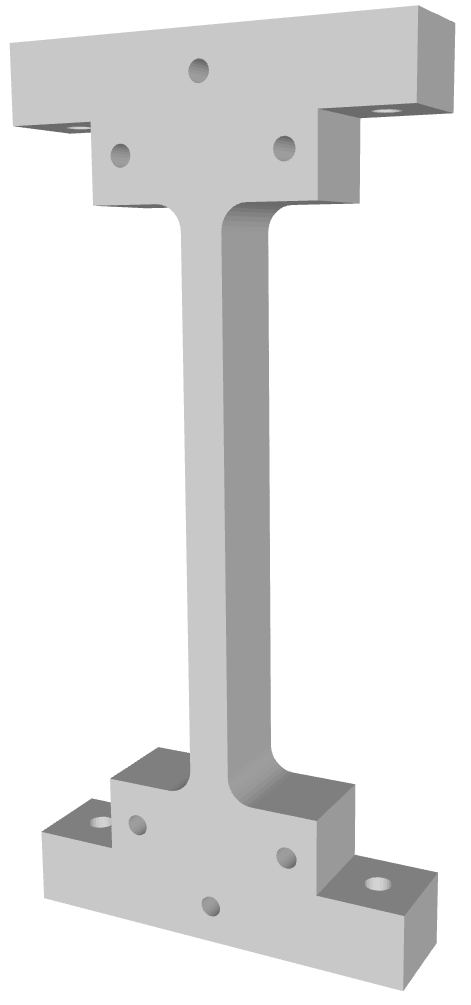
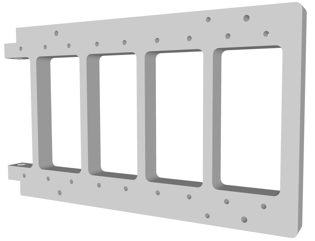
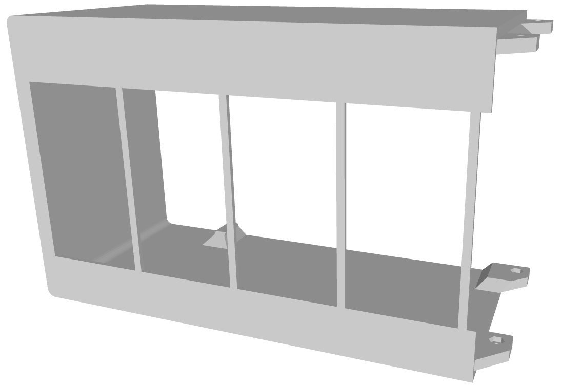
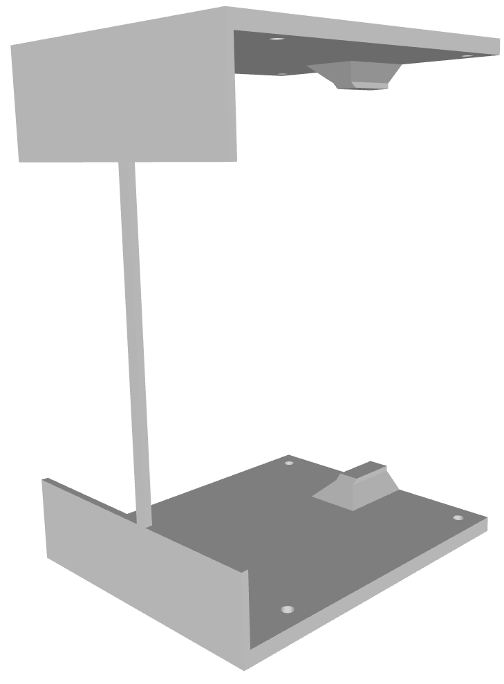
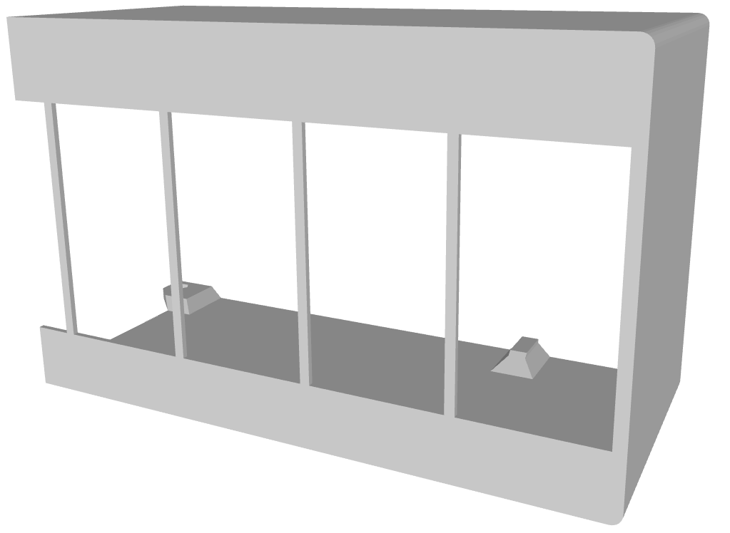
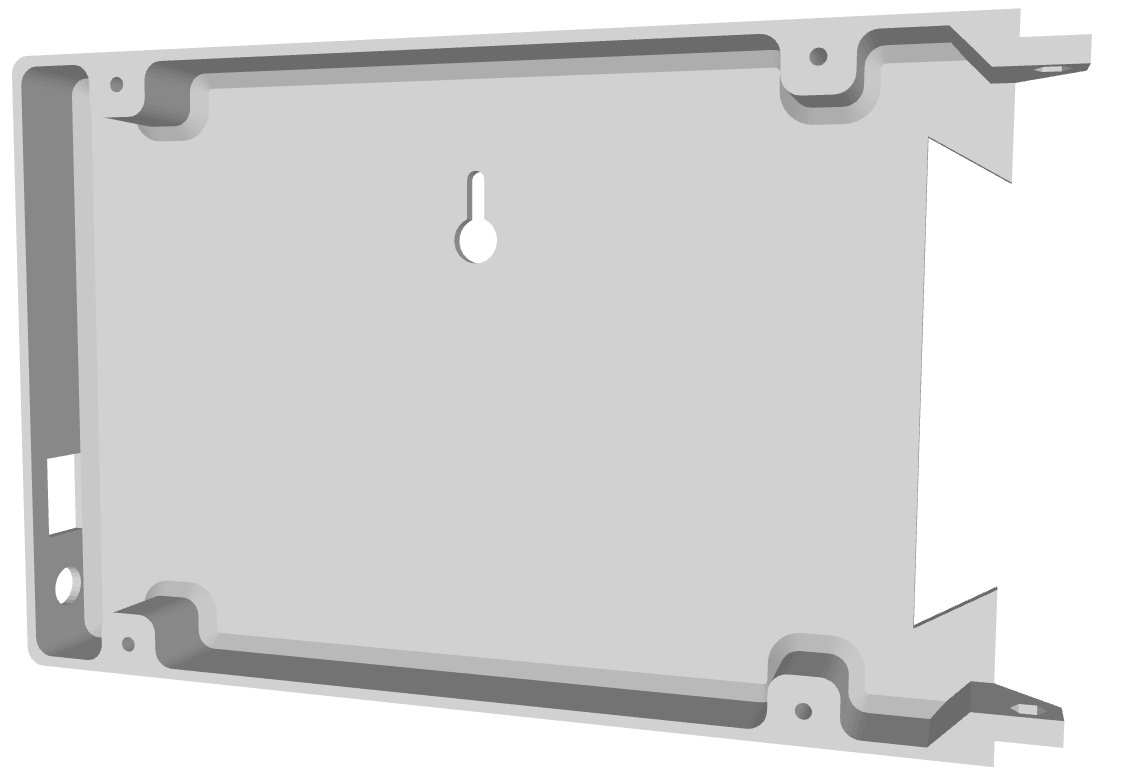
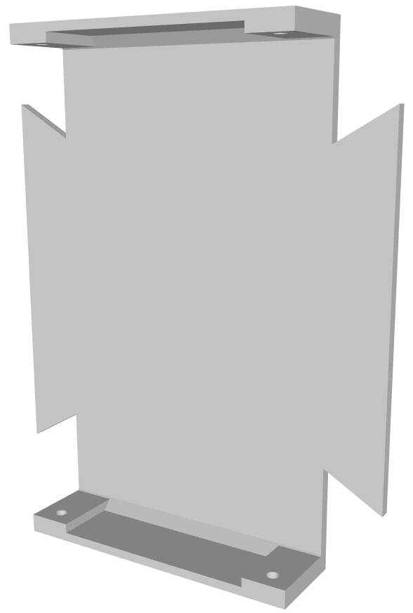
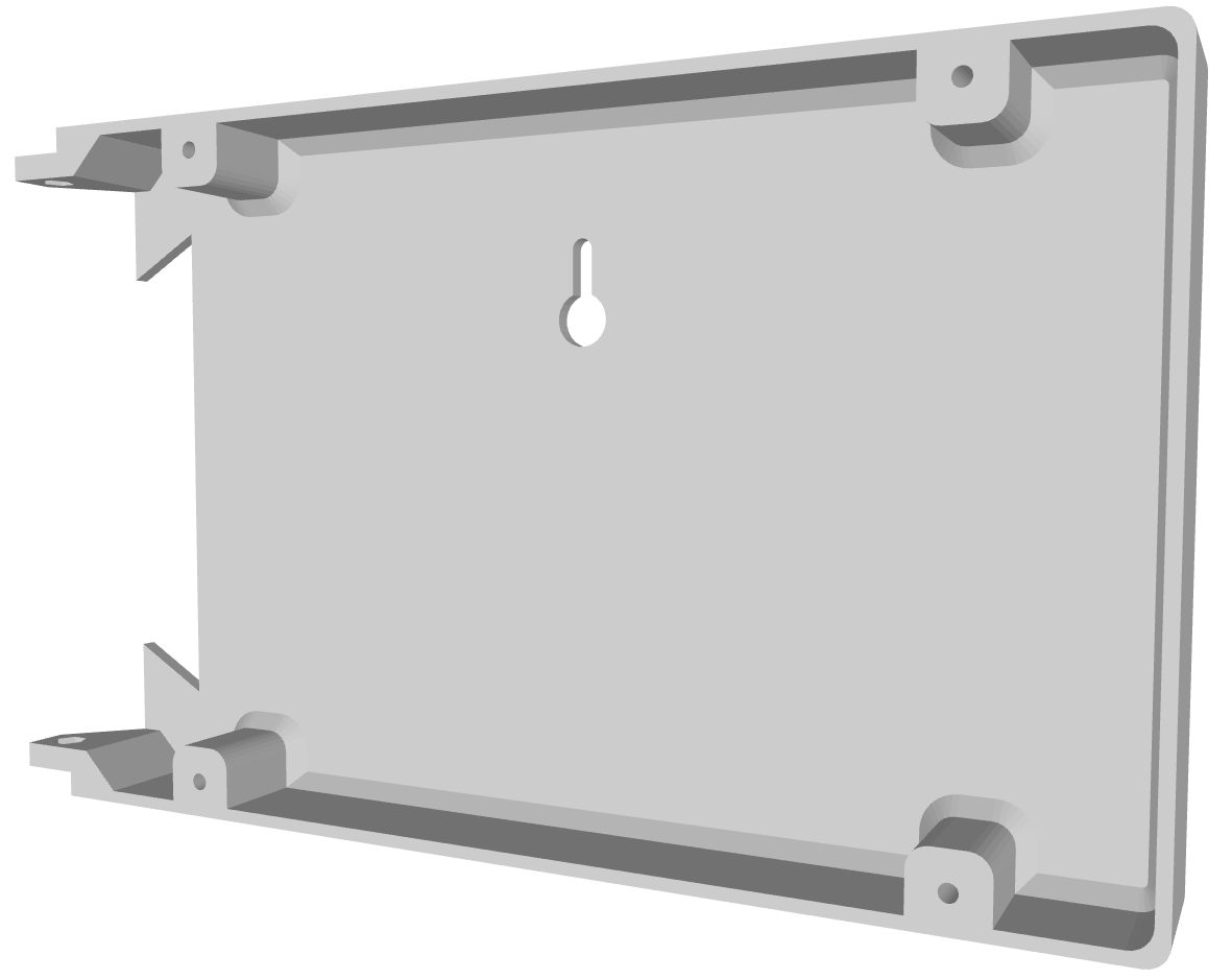
Upstream's renders of the 10-unit parts. Shorter cases have shorter Left and/or Right pieces.
1 · Solder the PCBs
×9Both views have the board's top edge up: that's the edge nearest U10 and the U4 chip, and U7 and U8 sit on the opposite edge. The numbers on the maps are the soldering order in the table. The board says Version 1.2 on the top side; the photos in stage 3 show an older version.
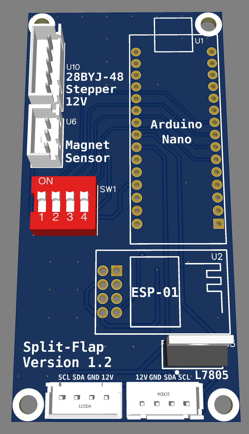
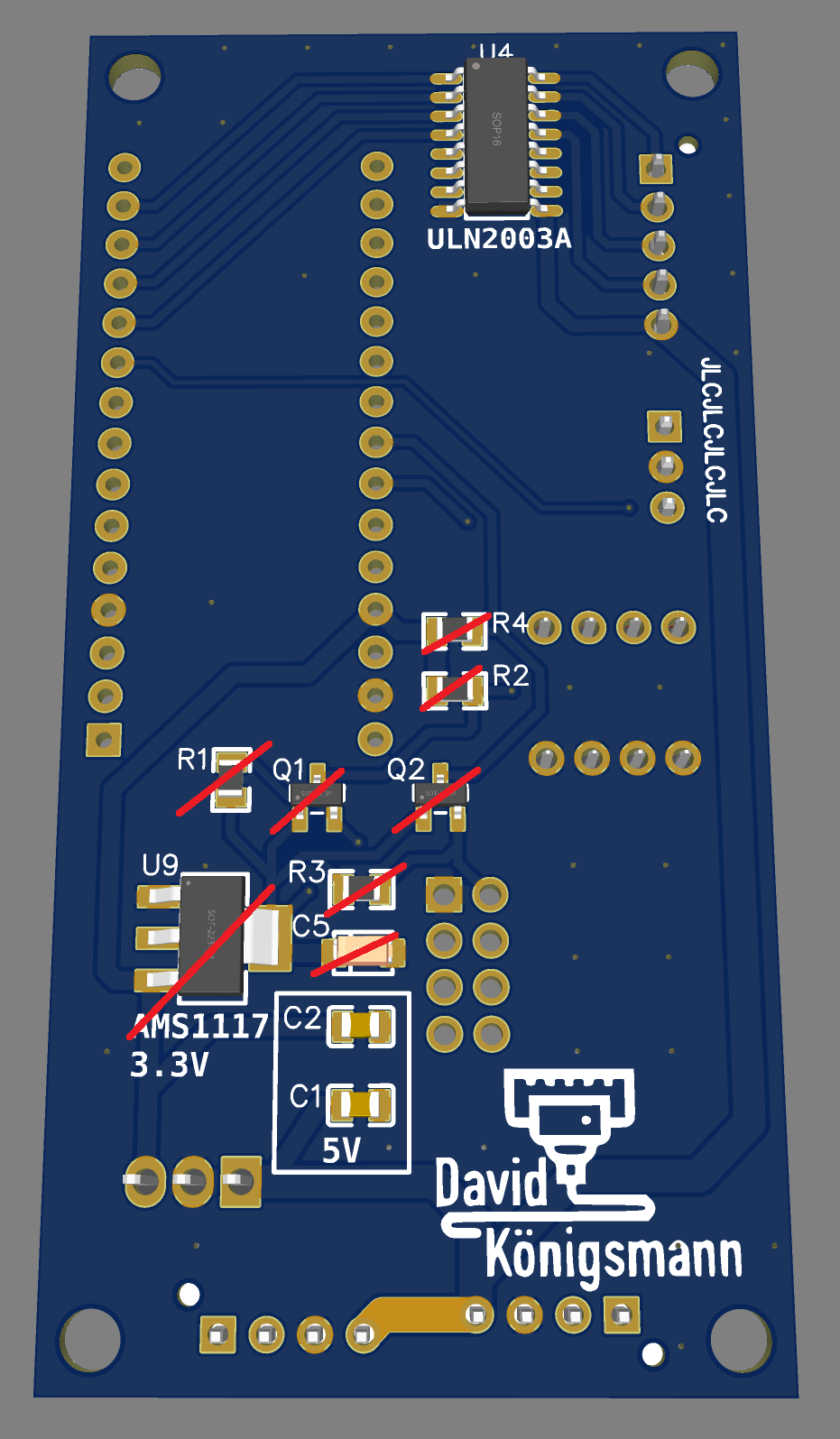
| # | Part | Ref | Side | Where | Which way round |
|---|---|---|---|---|---|
| 1 | ULN2003A | U4 | Bottom | Near the top edge | Dot and pin 1 at the top left, as in the bottom view |
| 2 | 100 nF | C2 | Bottom | Upper spot in the box marked 5V | Either way |
| 3 | 330 nF | C1 | Bottom | Lower spot in the box marked 5V | Either way |
| 4 | DIP switch | SW1 | Top | Left edge, below U6 | Marked ON edge toward U6, switch 1 on the left |
| 5 | 1×15 headers × 2 | U1 | Top | The two long rows, right side | Either way. The Nano's USB end goes to the top edge |
| 6 | XH 5-pin | U10 | Top | Top left corner | The peg under the socket only fits one way |
| 7 | XH 3-pin | U6 | Top | Left edge, below U10 | No peg: same way round as U10 |
| 8 | XH 4-pin × 2 | U7, U8 | Top | Bottom edge | The peg under each socket only fits one way |
| 9 | L7805 | U3 | Top | Above U8, right side | Upright, metal tab toward the Nano |
-
Don't lay it flat, even though the older boards in the stage 3 photos have it that way: its metal tab would rest on the empty ESP-01 pads.
-
Check with the meter which jack tab is the centre pin, and that your supply is centre-positive.
| Socket | Pins, in order |
|---|---|
| U7 (printed on the board) | Left to right: SCL, SDA, GND, 12V |
| U8 (printed on the board) | Left to right: 12V, GND, SDA, SCL |
| U6 (not printed) | From the U10 end down: 5V, GND, signal |
| Nano | SDA is A4, SCL is A5 |
2 · Drums and flaps
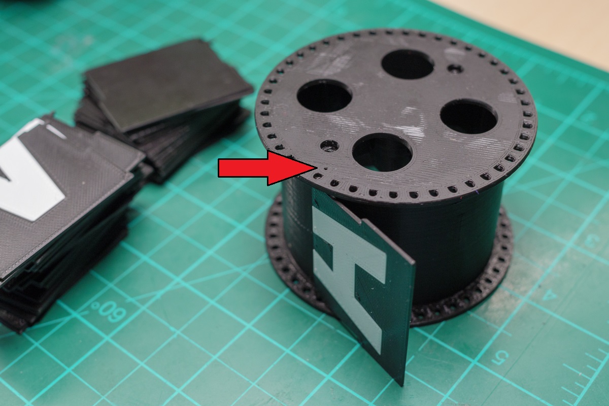
×9FlapDrumOuter is the long open cylinder. FlapDrumInner is the disc with spokes, four large holes and the motor hub. Each has a ring of 45 flap holes, and the flaps hang between the two rings.
The two drum halves are the CAD parts. The magnet and flaps are simplified shapes. Yellow marks the parts a step moves, orange what it adds.
-
2× M2 insert
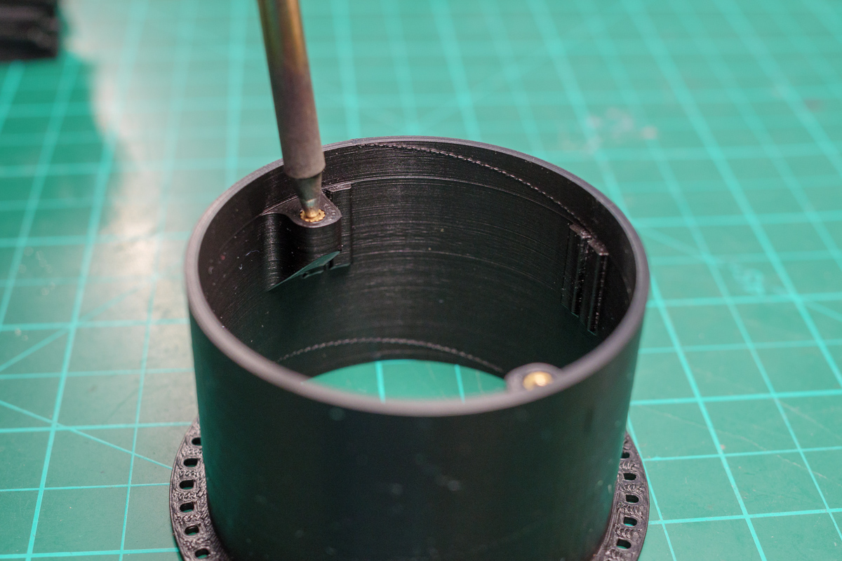
-
On most KY-003 boards the middle pin is +, so a straight-through cable would reverse the power. Go by the labels on your board. If only S and − are marked, the unmarked pin is +.
-
-
Flaps go in by file number, so keep the plates separate. If you printed the five
Flaps PTplates, they are the whole set. If you printed upstream's flaps, take 1, 14, 15, 24, 25, 28–31 and 41–45 fromFlaps PTinstead. The drum then reads: blank A–Z Ã Ç É 0–9 Á . TikTok Instagram Facebook. - 2× M2×8
3 · Unit assembly
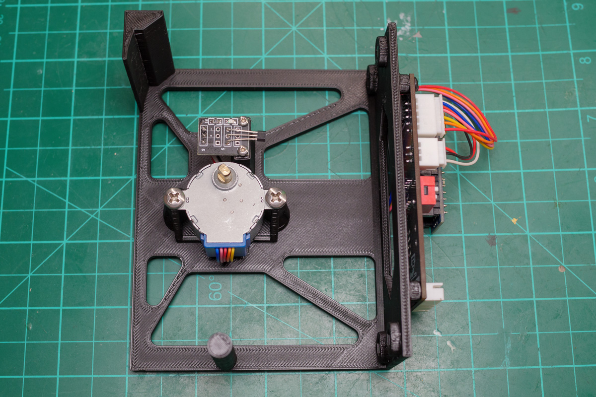
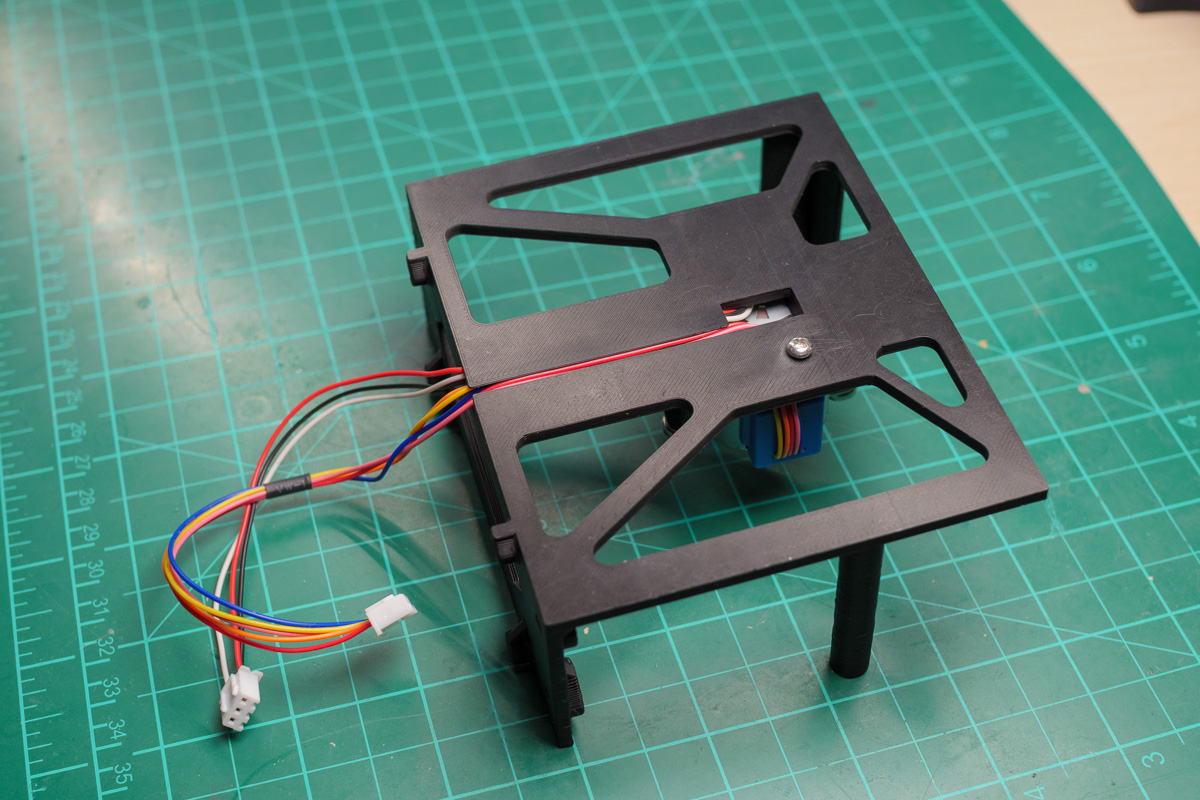
×9UnitFrame has a flat base, a side wall for the motor, and an upright PCB plate at one end. The PCB goes on the outside of that plate. Later the plate is screwed to the middle frame and the PCB pokes through a window.
The frame and drum are the CAD parts. The motor, sensor and board are simplified shapes placed on the frame's real mounting holes. The flaps and cables are left out.
- 2× M3 nut
- 2× M4×8
- 2× M2×4
-
- 2× M3×6
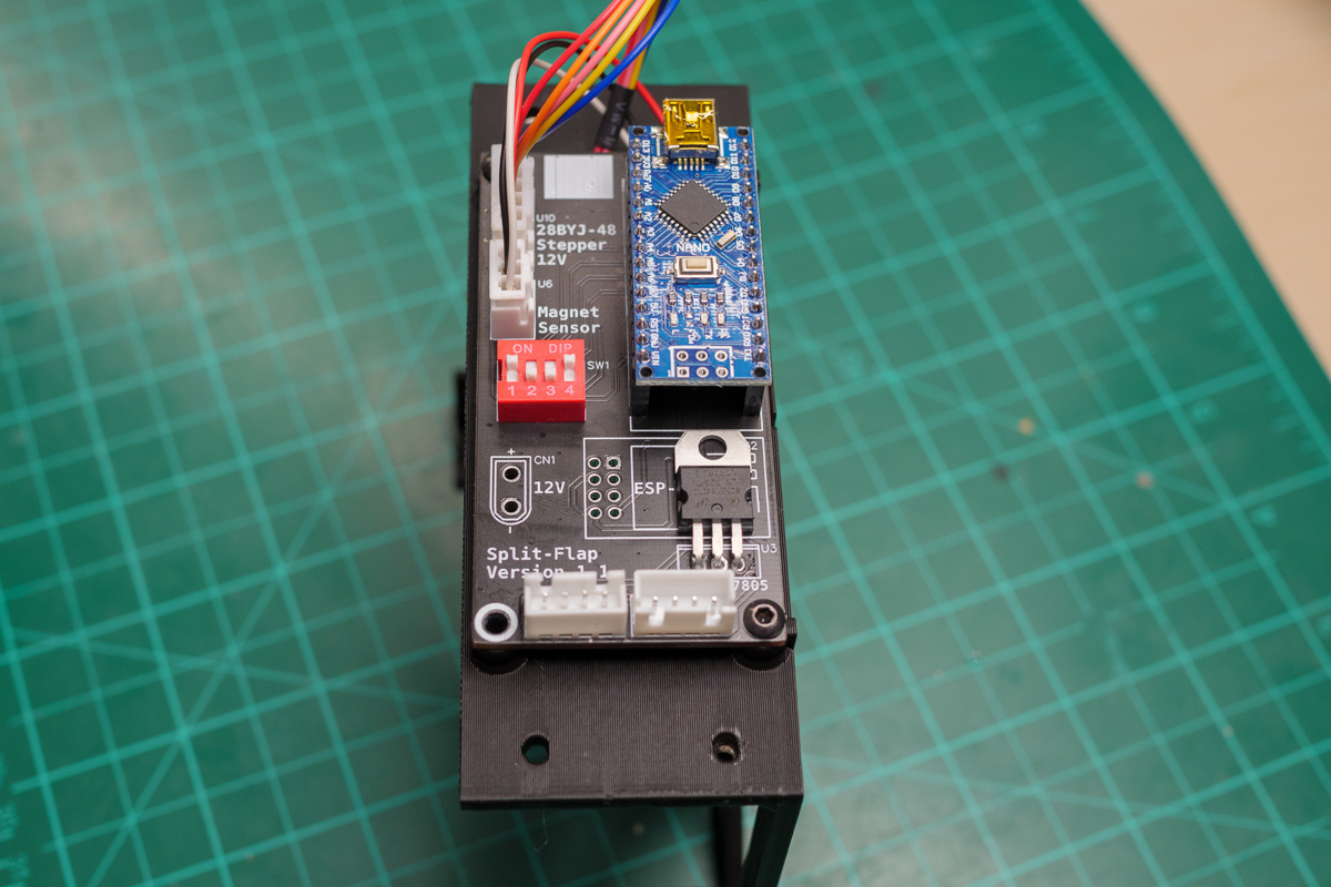
An older board. Yours says Version 1.2, has no 12V terminal, and has the 7805 upright.
4 · First unit test
one unit, before building the restOn the PC, in a terminal opened in this repo's folder (the one with platformio.ini), with the Nano on USB and the unit on 12 V through the power lead in U8. Stop pio device monitor with Ctrl+C before each upload, because it holds the port.
-
If the upload fails with a sync error, the Nano has the newer bootloader: change
boardtonanoatmega328newin theunitandoffset_toolsections ofplatformio.ini. -
If a neighbouring flap shows, repeat step 1 with a larger or smaller offset. About 45 steps is one flap.
5 · Case
files for 9 unitsRead this first
- Front is the side where the flaps show. Back is the side the PCBs face. Left and right are always as seen from the front, so when you work from the back, the left end is on your right.
- The case is three layers, front to back: front cover (an open box), middle frame (a flat 15 mm plate with one window per unit) and back cover (a shallow tray). They sit edge to edge, held by screws; nothing slides inside anything.
- Each layer is printed as Left, Center and Right pieces. At each seam, the Center piece's tabs lie over the ends of the Left or Right piece, in the top and bottom edges. A joint screw goes in from the outside top or bottom edge, through the Center tab, into a nut sitting in a hex pocket inside the Left or Right piece. The pocket opens on the inside of the case.
- Work on a soft cloth. Melt inserts at about 200 °C, push straight, and stop when they're flush.
| Middle frame hole | Where (windows counted from the left, seen from the front) | Used for |
|---|---|---|
| Counterbored on the back | 4 around each window: 2 just above, 2 just below | Units: M3×16, 2 per window (the diagonal pair with nuts behind) |
| Counterbored on the back | 6 in the outer rows, close to the top and bottom edges, between windows 1–2, 4–5, 8–9 | Front cover: M3×16 into its inserts |
| Plain 4 mm, no counterbore | 8 in the outer rows, above and below windows 1, 3, 6, 9 | M3 inserts. The back cover screws into these |
| Vertical, in the top and bottom edges | At the two seams, through the Center piece's tabs | Joints: M4×20 + M4 nut |
Drag to turn the model, pinch or scroll to zoom. Click a step again to replay it. Yellow marks the parts a step moves, orange the screws, nuts and inserts it adds.
-
8× M3 insert
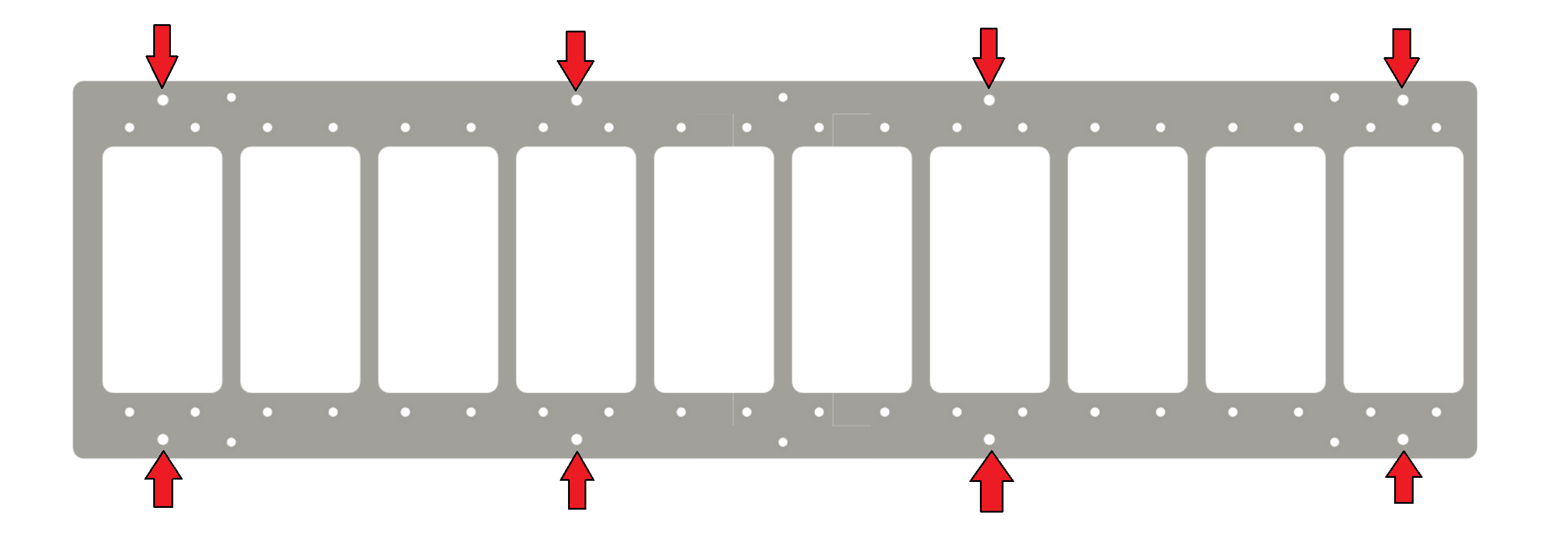
Upstream's drawing for the 10-unit frame. On a shorter case the window numbers above are what counts. -
4× M4 nut4× M4×20A bit of tape over a pocket keeps its nut in while you turn the frame over.
-
2× M3×16 per unit
-
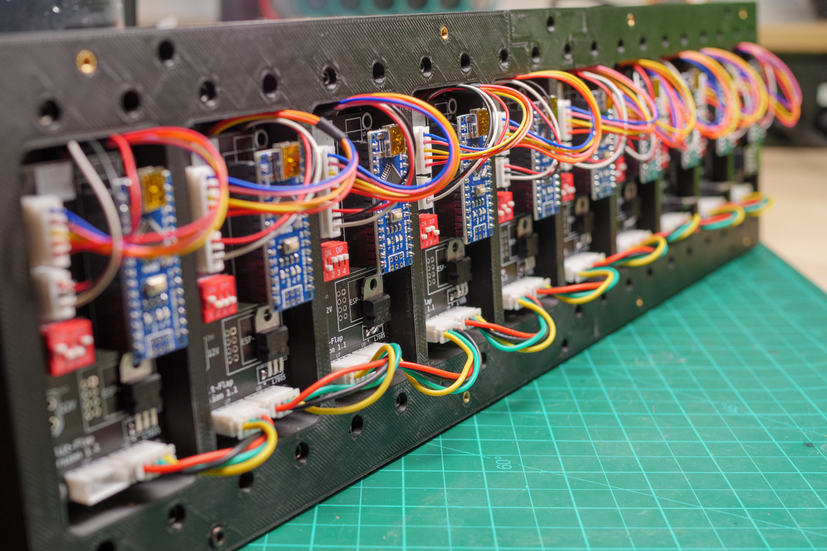
Seen from the back, so unit 0 is on the right. This shows the order only: find U7 and U8 by the labels printed on each board. Check each cable before any power, because a reversed one puts 12 V on SCL. Meter between the two units: left leg of the 7805 to left leg of the 7805, Nano A4 to A4, A5 to A5, and GND to GND must all beep.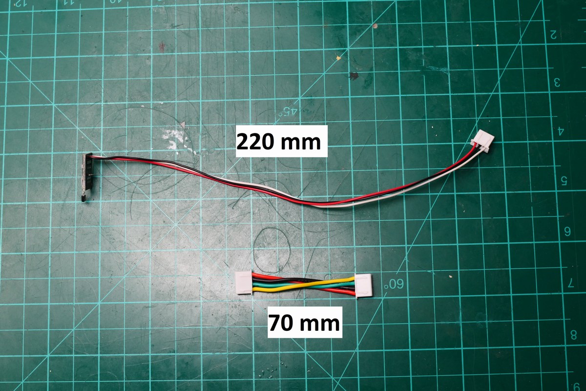
Upstream's cables, shorter than yours. Any slack in the 100 mm and 300 mm cables tucks into the case. -
6× M3 insert
-
8× M3 nut8× M3×8
-
6× M3×16
-
4× M3 nut4× M3×8
-
8× M3×16
6 · Power and ESP32
Option B inhardware/wiring.mdThe same wiring as text
Power (power lead in unit 0's U8)
  DC jack + ── switch ──┬── lead 12V
                        ├── buck IN+
                        └── 1000 µF +
  DC jack − ────────────┬── lead GND
                        ├── buck IN−
                        └── 1000 µF − (striped side)

  buck OUT+ ──┬── ESP32 VIN
              └── level shifter HV
  buck OUT− ──┬── ESP32 GND
              └── level shifter GND

Signals
  lead SDA ── shifter HV1    LV1 ── ESP32 GPIO21
  lead SCL ── shifter HV2    LV2 ── ESP32 GPIO22
                             LV  ── ESP32 3V3
7 · All units
addresses and full testAddresses come from the DIP switch, read at power-up: 0x10 plus the switch value, with switch 1 as the highest bit. To change one, set it and power the unit off and on again. Reflashing the ESP32 later means taking the back cover off.
| Unit (left → right) | DIP 1 2 3 4 | Address |
|---|
Troubleshooting
hardware faults, by symptom| Symptom | Check |
|---|---|
| No 5 V at the Nano header, or the 7805 gets hot | Disconnect the power. Check the 7805's direction (stage 1, step 5), then repeat the meter check for shorts (step 6). Look for solder bridges on U4. |
| Upload to a Nano fails with a sync error | The Nano has the newer bootloader: set board to nanoatmega328new (stage 4, step 1). If the port is busy, stop pio device monitor first. |
| The sensor's LED never lights when the magnet is near | The hall cable is wired by position and not by function, so the sensor has no power (stage 2, step 2). Check that the board has 12 V. |
| A neighbouring flap shows after homing | Run the offset tool again for that unit (stage 4, step 1). One flap is about 45 steps. |
| A drum keeps turning and never homes | The sensor doesn't see the magnet. Check that the magnet's marked face points out (stage 2, step 4), that it passes close to the sensor (stage 3, step 6), and that the sensor is plugged into U6. A unit gives up after 3 turns. See also step 4 of the bring-up list in hardware/wiring.md. |
The scan shows one unit as MISSING | Check its DIP switch against the table in stage 7, then power it off and on, because the switch is only read at power-up. Check its bus cable (stage 5, step 6) and that its Nano is fully seated. The Nano must run this repo's unit firmware. |
| No unit answers the scan | SDA and SCL are swapped, a GND is missing, or the level shifter is wired wrong. Compare every wire with the drawing in stage 6. |
| Units stutter or restart when they all move | The 12 V rail is sagging: each 7805 needs at least 7 V in. Use a 12 V supply of 3 A or more, fit the 1000 µF capacitor, and keep the power wires short (stage 7, step 2). |
| The web page is blank or shows 404 | The filesystem wasn't uploaded: pio run -e master -t uploadfs (stage 6, step 4). |
| Wi-Fi, accounts, tokens or wrong counts | See Troubleshooting in README.md. |